|
| |
|
ERC Vision, Goals and Research Strategy: |
VISION
In 1996,
the NSF/SRC
Engineering Research Center (ERC) for Environmentally Benign Semiconductor
Manufacturing was created as a result of a joint initiative between
the University of Arizona
(lead institution), the Massachusetts Institute
of Technology, Stanford University,
and the University of
California-Berkeley
with co-sponsorship from the National Science
Foundation (NSF) and the Semiconductor Research Corporation (SRC).
The ERC's goal was to create the science,
technology, and educational methods needed to lead the semiconductor industry to a new
era of environmentally benign manufacturing. When the ERC "graduated"
from the NSF's Engineering Research Center program in 2006, the ERC continued
under sponsorship of the SRC jointly with SEMATECH/ISMI (2006-2011). The
ERC has continued its partnership with the Semiconductor Research Corporation (SRC)
throughout, and continues its firm commitment to developing its goals and
objectives.
GOALS AND OBJECTIVES
- Develop novel strategic solutions to existing environmental, safety and health (ESH)
problems in semiconductor manufacturing.
- Create new and effective environmentally benign manufacturing processes.
- Demonstrate the positive impact of design for environment on all aspects of
semiconductor manufacturing
- Develop innovative education programs in which environmental factors are integral parts
of the curriculum.
Our specific objectives for achieving these goals were to:
- Develop a methodology for incorporating Environment, Safety & Health (ESH) factors
as design parameters in the development of new processes, tools, and protocols for
semiconductor manufacturing. The emphasis is on an "integrated approach,"
where interactions among processes are considered, and on "process optimization"
for waste minimization. rather than relying on abatement and "end-of-the-pipe"
treatments.
- Demonstrate this methodology by applying it to selected manufacturing process groups
that are of significant ESH concern.
- Integrate the Center activities with academic programs to provide unique learning
opportunities for undergraduate and graduate students
- Extend the education mission to include continuing education and short courses for those
in industry who wish to update their training in this area, and outreach to high school
teachers to improve science and math instruction and make teachers aware of employment
opportunities in the environmental and semiconductor industries.
- Provide a technical forum for experts from industry, research institutions, and
government agencies to exchange ideas and information on ESH concerns in semiconductor
manufacturing. These exchanges will be on a proactive, preventive, non-regulatory,
and pre-competitive basis.
|
 |
RESEARCH
STRATEGY AND ORGANIZATION
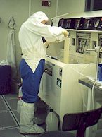 |
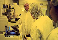
Environmental factors are often not included in the design and development
of new tools and processes in the semiconductor industry. Integrating Design
For the Environment into new processes and tools for the
industry is the technical driver and the common theme of the Center’s
research. The Center’s interdisciplinary research efforts involve
14 universities and 11 different academic disciplines.
The semiconductor industry is a very fast-moving industry, one which creates many
opportunities for innovation and implementation of changes. The fast pace also presents a
major challenge in planning and conducting long-term research. One challenge is to strike
the right balance between long-term development, short-term relevance, and application to
the present problems. The Center’s research strategy is to maintain this balance
and promote a mix of projects and activities ranging from high-risk, high-payoff research
to smaller projects with more immediate applications. |
Originally organized in thrusts built around semiconductor manufacturing
processes [Thrust A (Back-End Processes), Thrust
B (Front-End), Thrust C (Factory Integration), and Thrust D
(Patterning)], the ERC's current core research and customized
projects are listed
below.
Annual reports, interim research reports and annual review meeting materials
are also listed below, and are available to SRC and ERC members only;
these materials are password
protected, privileged information and not
for distribution. SRC members can
access ERC research information via the SRC website:
http://www.src.org.
|
SRC-ERC CORE PROJECTS:
2015 - 2017 |
|
|
425.036 |
Administration of SRC Engineering Research Center for Environmentally Benign
Semiconductor Manufacturing
Farhang Shadman, ERC Director |
|
425.046 |
Alternative Etchants for Magnetic Materials
Faculty participant: Jan Pei-Chen
Chang (University of California-Los Angeles) |
|
425.048 |
Bioaccumulation, Biopersistence, and Toxicity of CMP Nanoparticles in
Mammalian and Aquatic Models (SRC 425.048)
Faculty participants: Rockford Draper (University of Texas/Dallas); Paul Pantano
(University of Texas/Dallas) |
|
425.049 |
Investigation of Speciation in III-V Wet Etching to Mitigate Hazardous
Product Formation (SRC 425.049)
Faculty participants: Anthony
Muscat (University of Arizona); Srini Raghavan
(University of Arizona) |
|
425.050 |
Understanding the Sorption Characteristics of III-V Wet Materials on CMP
Nanoparticles and Evaluate their Environmental Impact using a Zebrafish Model (SRC 425.050)
Faculty participant: Andre Nel (University of California/Los Angeles) |
|
425.051 |
Understanding the Physicochemical Properties, Behavior and Toxicity
Threshold Limit of Bound and Unbound Engineered Nanomaterials (SRC
425.051)
Faculty participant: Shyam Aravamudhan (North Carolina A&T) |
|
425.052 |
Aquatic Fate and Toxicity of III/V Semiconductor Materials in the
Presence of Chemical-Mechanical Planarization Nanoparticles (SRC
425.052)
Faculty participants: Reyes Sierra (University of Arizona); Paul Westerhoff (Arizona
State University)
|
| |
|
|
SRC-ERC CORE PROJECTS:
2012 -
2014 |
|
|
425.036 |
Administration of SRC Engineering Research Center for Environmentally Benign
Semiconductor Manufacturing
Farhang Shadman, ERC Director |
|
|
425.036 |
* Preparation and Characterization of Model
CMP Nano-Particles
Faculty participants:
Reyes Sierra (Lead PI), Jim Field, and Farhang Shadman, University of
Arizona
* Methods for Reducing the Usage of UHP Gases in Fabs
Faculty participants:
Farhang Shadman (Lead PI), Jim Field, and Reyes Sierra, University of
Arizona |
|
|
425.037 |
Cell-Based Toxicity
Assay-on-Chip for the Next-Generation CMOS Technology
Faculty participants: Shyam
Aravamudhan, North Carolina A&T State University (Lead PI); Marinella Sandros, UNC/Greensboro; Ethan Taylor, UNC/Greensboro; Shanthi
Iyer, NC A&T |
|
|
425.038 |
Non-PFC Plasma Chemistries
for Patterning Complex Materials and Structures
Faculty participants: Jane Pei-Chen
Chang, University of California-Los Angeles (Lead PI) |
|
|
425.039 |
'Pad-in-a-Bottle':
Planarization with Slurries Containing Suspended Polyurethane Beads
Faculty participants: Ara
Philipossian (Lead PI), University of Arizona; Duane Boning, Massachusetts
Institute of Technology |
|
|
425.040 |
Detection of Engineered
Nanomaterials at Semi-Conductor Facilities and Consumer Products
Faculty participants: Paul
Westerhoff (Lead PI), Arizona State University; Jonathan Posner, University
of Washington; Pierre Herckes, Arizona State University; James Ranville,
Colorado School of Mines; Chris Higgins, Colorado School of Mines |
|
|
425.041 |
Interactions of Chemical
Mechanical Planarization Nanoparticles with Model Cell Membranes:
Implications for Nanoparticle Toxicity
Faculty participant:
Kai Loon Chen (Lead PI), Johns Hopkins University |
|
|
425.042 |
Dispersion,
Bioaccumulation, and Mechanisms of Nanoparticle (NP) Toxicity
Faculty participants:
Steven Nielsen (Lead PI), Rockford Draper,
Paul Pantano, Inga Musselman, and Gregg Diekmann, University of Texas-Dallas |
|
|
425.043 |
ESH-Friendly Cleaning and
Rinsing of Multi-Material Surfaces and Structures
Faculty participants: Farhang
Shadman (Lead PI), Srini Raghavan, and Manish Keswani, University of Arizona |
|
|
425.044 |
Computer-Aided Design of
Nanomaterials with the Desired Bioactivity and Safety Profiles
Faculty participants: Alexander
Tropsha (Lead PI), and Denis Fourches, University of North Carolina-Chapel Hill |
|
|
425.045 |
Develop Externally
Validated QNAR Models that can be Reliably Used to Prioritize Nanoparticles
for Biological and Safety Studies
Faculty participants:
Alexander Tropsha (Lead PI), and Denis Fourches, University of North Carolina-Chapel Hill |
|
|
425.046 |
Alternative Etchants for Magnetic Materials
Faculty participant: Jan Pei-Chen
Chang, University of California-Los Angeles (Lead PI) |
|
|
425.047 |
Initial Sorption and Toxicity
Screening of III/V Ions
Faculty participants: Farhang
Shadman (Lead PI), and Reyes Sierra, University of Arizona |
|
|
2324.001 |
Solutions Irradiated with Megasonic Waves
Faculty participants: Srini
Raghavan (Lead PI), and Manish Keswani, University of Arizona |
|
|
2481.001 |
N(2)O Abatement: Reaction
Mechanisms and Methods for Improving Efficiency
Faculty participants: Farhang Shadman (Lead PI), University of
Arizona, and Jost Wendt (University of Utah) |
|
|
CUSTOMIZED HVmM PROJECTS
(Co-sponsored by Intel and ERC):
2012-2014 |
|
|
Attenuation of CMP Nanoparticles by
Wastewater Sludge
Jim Field, University of Arizona; Reyes Sierra, University of Arizona |
|
|
Natural Resource Conservation in
Semiconductor High Volume Manufacturing by Waste Brine Minimization and
Solids Recovery by Membrane Distillation
Wendell Ela, University of Arizona |
|
|
Reclamation of Sulfuric Acid from
Spent Piranha Solutions and Piranha Generated Wastewater (Novel Technologies
for Lowering Water Usage and Waste Discharge
James Farrell, University of Arizona; [Carl Geisert, Intel] |
|
|
Recovery of Solvents from
Semi-Aqueous Waste Streams Generated from Various Semiconductor Processing
Steps
Srini Raghavan, University of Arizona; Manish Keswani, University of Arizona |
|
|
Removal of Inorganic Nanoparticles
in CMP Effluents Using Porous Media Filtration
Reyes Sierra, University of Arizona |
|
|
Treatment of High Fluoride, High
Ammonia Wastewaters using Fluidized Bed Crystallization and Electrochemical
Ammonia Destruction
James Farrell, University of Arizona; [Allen Boyce, Intel] |
|
|
|